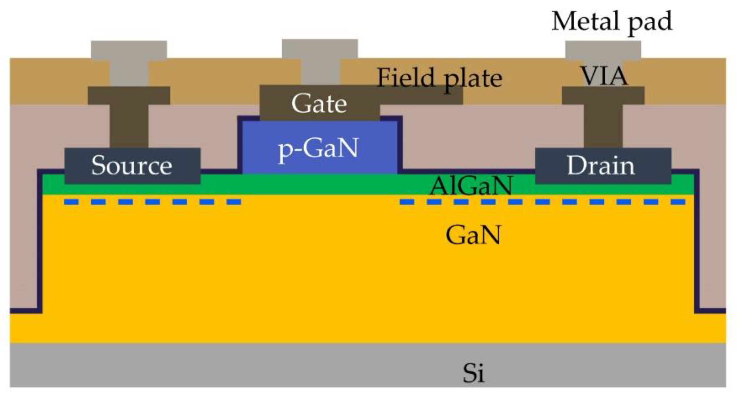
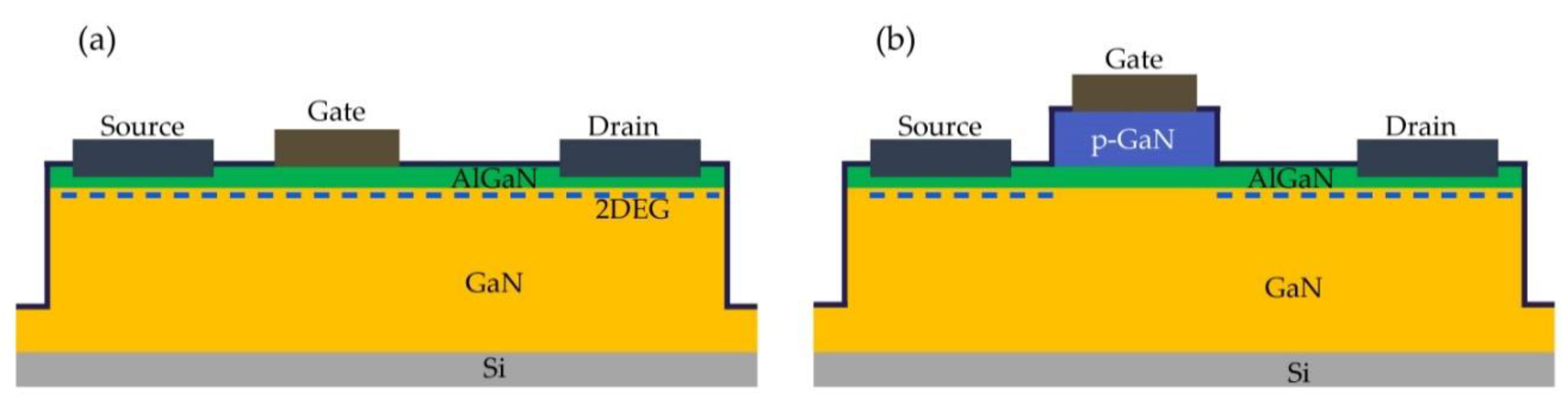
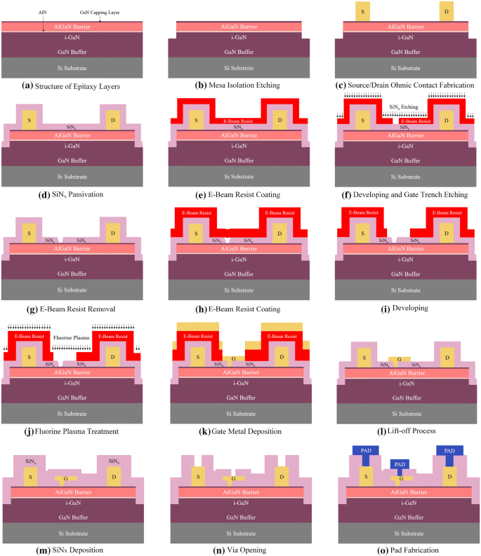
Gan Hemt Process Flow
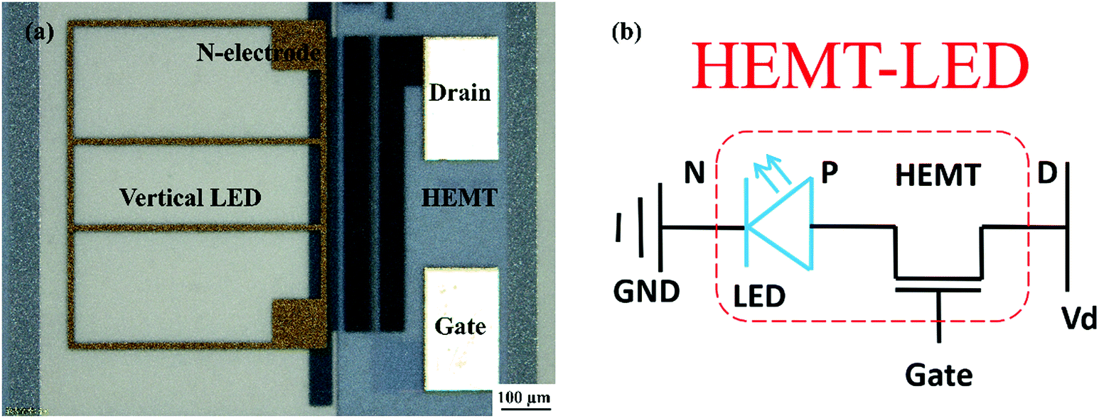
Efficiency Improved By Monolithic Integration Of Hemt With Vertical Structure Leds And Mg Doping On Dry Etched Gan Journal Of Materials Chemistry C Rsc Publishing

Revisiting The Seminal Apa Optics Gan Hemt Patent Techinsights
Highly Sensitive Algan Gan Hemt Biosensors Using An Ethanolamine Modification Strategy For Bioassay Applications Rsc Advances Rsc Publishing
Snfexfab Stanford Edu Sites G Files Sbiybj8726 F Sections Diplayfiles Engr241 Final Report Sj Al 1819win Pdf
Micromachines Free Full Text Gallium Nitride Gan High Electron Mobility Transistors With Thick Copper Metallization Featuring A Power Density Of 8 2 W Mm For Ka Band Applications Html
Examples Research Service Centers
In this paper, a consistent DC to RF modeling solution for Al gallium nitride (GaN)/GaN high electron mobility transistors is demonstrated that is constructed around a surface-potential-based core.
Gan hemt process flow. With Cree's GaN process, our mutual customers have access to a powerful MMIC design solution in an integrated flow for leading-edge, high-power applications," said Anitha Swaminathan, foundry program manager with Agilent's EEsof EDA division. GaNPX packaging for extreme speed and current -Near chipscale embedded package -High current density & low profile -Optimal thermal performance -Extremely lo. We develop a physics based analytical model for AlGaN/GaN high electron mobility transistors (HEMT and MOS-HEMT) to study the I- Vcharacteristics, current transfer characteristics, transconductance.
For comparison, Titanium (Ti/Al/Ti) gate devices are also fabricated using the same process flow except the gate topology which is double T-shaped gate for Ti/Al/Ti. Hydrogen (H 2) and nitrogen (N 2) act as the carrier gases, with trimethylgallium (TMGa), Trimethylaluminium (TMAl) and ammonia (NH 3) as the sources. For GaN HEMTs on silicon substrate, RF performance of 12 W/mm at 2 GHz and 7 W/mm at 10 GHz have been re-ported 7, 8.
The NRL “Gate after diamond” approach has demonstrated % reduction in self-heating. Symmetric device structures are considered. This webinar represents a continuation of a previously presented parameter extraction methodology for GaN HEMT devices.
This comparison highlights the huge differences in design and manufacturing process and their impact on device size. E-mode, p-GaN, HEMTs, GaN on Si. Except the demonstration of high threshold voltage (V th) of 4.3V, the process window of the p-GaN residual thickness to.
Introduction Gallium Nitride (GaN) is suitable for high electron mobility transistors*1 (HEMTs), because the breakdown voltage and electron velocity of GaN are higher than those of Gallium Arsenide (GaAs) and Silicon (Si). In comparison to GaAs and Si technologies, less know-how exists for the integration of a via hole process in. The GaN HEMT process technology include a GaN cap layer to control surface charges and suppress current collapse, 6 μm.
A high-electron-mobility transistor (HEMT), also known as heterostructure FET (HFET) or modulation-doped FET (MODFET), is a field-effect transistor incorporating a junction between two materials with different band gaps (i.e. OMMIC Innovating with III-V’s 02/04/15 7. The buffer layers separating the Si substrate from the GaN layer limits the efficiency of bottom side cooling.
The effects of near-surface processing on the properties of AlGaN/GaN heterostructures were studied, combining conventional electrical characterization on high-electron mobility transistors (HEMTs), with advanced characterization techniques with nanometer scale resolution, i.e., transmission electron microscopy, atomic force microscopy (AFM) and conductive atomic force microscopy (C-AFM). High Etch Selectivity of GaN over AlGaN 0 Samco solved the selectivity issue by using a small flow of an additive gas (“Gas X”) in a chlorine-based gas plasma mixture. The absence of p-n junctions in lateral GaN-on-Si HEMTs prevents these devices from avalanche breakdown.
The Cree PDK, developed for use with Advanced Design System (ADS) from Agilent Technologies, Inc., can enable radio-frequency (RF) and microwave designers to shorten the development cycle for monolithic microwave integrated circuits (MMIC) used in high-power, high-performance electronic systems, resulting in a highly productive design flow. OMMIC Innovating with III-V’s 02/04/15 11 OMMIC CONFIDENTIAL 15 Lg = 100 nm 0 100 0 300 400 500 600 700 800 900 0 5 10 15 25 30 Vds. 36 · Low Capacitance Gate Process for E-band GaN HEMTs INOCOMMUNICATIONS 1.
This MMIC process includes MIM capacitors, inductors, air bridges, metallic resistors, via through the substrate and two metal layers for interconnections. Figure 1 is the three-dimensional schematic of FPL HEMT, FBL HEMT, and Conv. After finishing the process of annealing wait 5 minutes to cool down.
Ideal for 5G wireless infrastructure and radar applications (PA and switches) 15, 28, and 48V PA operations. –Low Ron due to high 2DEG density 12with n s ~9x10 cm-2 and high mobility (~00 cm2/V.s) –High breakdown because of high bandgap (3.4 eV) –Low capacitance :. Backside processes are especially often challenging for GaN technologies due to the types of substrate material used.
In a today´s world of semiconductor devices silicon transistors dominate, while GaAs-based high mobility transistors (HEMTs) and heterojunction bipolar transistors (HBTs). 3, 4 Firebird High Value Problems (HVP):. (b) Post-ICP etch with exposed Si substrate.
C Fabrication Process of AlGaN/GaN HEMT 101 D De-embedding 105 Bibliography 113 Acknowledgement 121 iv. We report on a novel fabrication process of GaN-on-Diamond high electron mobility transistors (HEMTs) and its resulting thermal performance enhancement over conventional GaN-on-SiC technology. High threshold voltage of around 1.6 V and current densities up to 400 mA/mm were obtained.
The second generation of this process implements diamond directly on GaN to serve both as a passivation layer and to increase the heat spreading effect. In this process, GaN devices are first fabricated on their epitaxial substrate (e.g. 0.25/0.4/0.5µm GaN HEMT Process.
2 Process flow for fabricating stretchable AlGaN/GaN HEMTs. GaN Systems GSB GaN HEMT 18 teardown reverse costing report published by System Plus 1. GaN growth on Si substrate technology is well-explored.
Low-voltage E/D-mode transistors, diodes, resistors. 42,44) Figure 1 shows a commercial GaN-on-Si p-GaN gate HEMT platform. TCAD-based Model Extraction Flow for GaN HEMT Devices.
After the usual wafer cleaning and inspection, an epitaxial layer must be grown to provide the required material characteristics necessary for HEMT and PHEMT devices. Sapphire or SiC) before being removed from the original substrate and bonded onto a high-thermal-conductivity diamond substrate at low temperature. Effects of process flows and device structures on the electrical properties of enhancement mode high electron mobility transistors (HEMTs) are investigated in this work.
AlGaN/GaN Lateral HEMT Devices • AlGaN/GaN High Electron Mobility Transistors feature :. Further, GaN-on-Si HEMTs are difficult to cool from the top due to the sensitivity of current conduction close to the device surface. An etch selectivity of 60:1 (GaN/AlGaN) is achieved, and the etch process is successfully stopped on the AlGaN interface without over-etching.
GaN technology is rapidly becoming of increased importance for many IC manufacturers. The 3MI process flow provides 3 levels of metal interconnect air-bridges and 3 capacitor density values to facilitate compact MMIC design. Sink layer for Gallium Nitride (GaN) high electron mobility transistors (HEMTs).
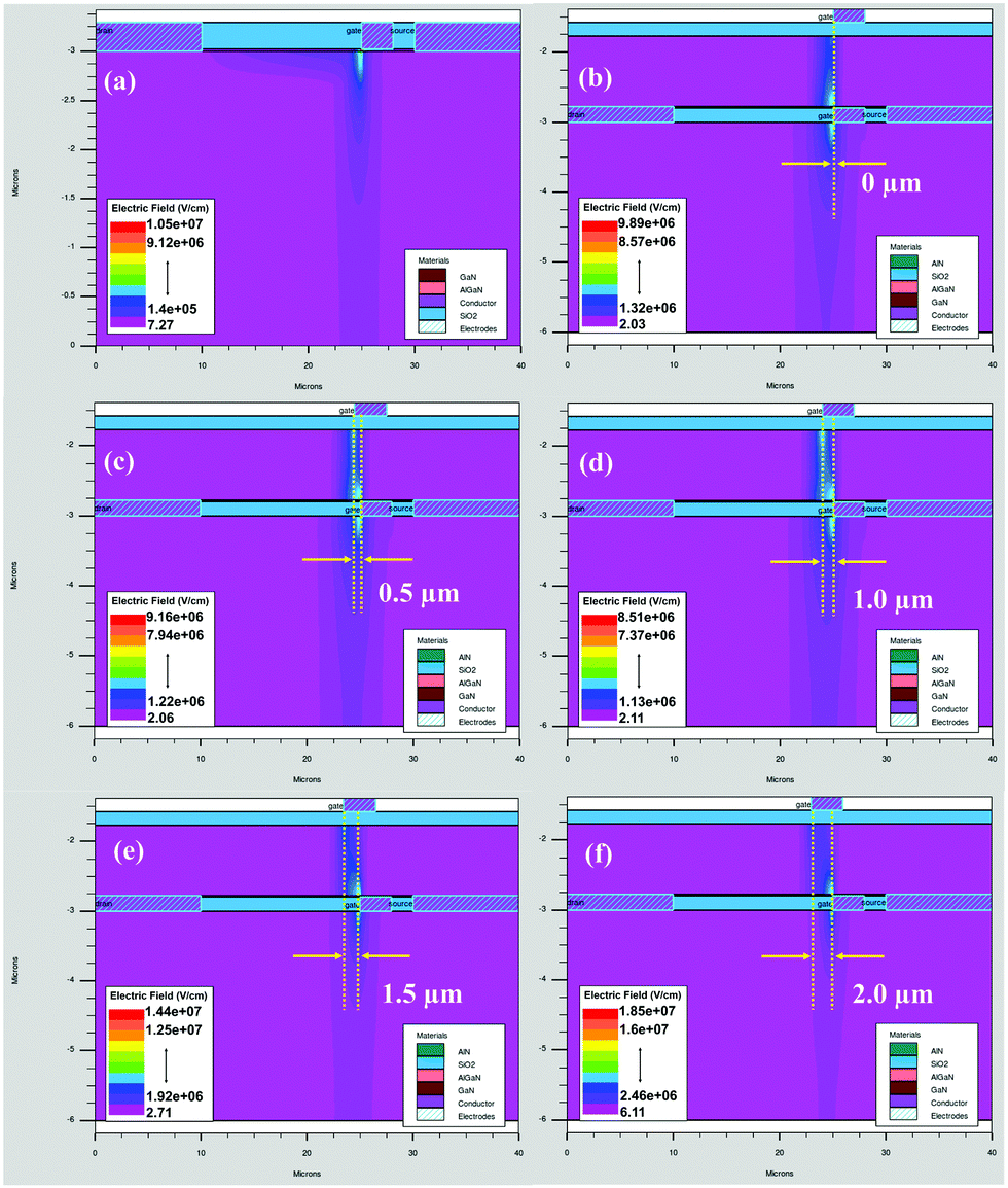
In this paper, we report a promising approach for the gate recess process with a suppressed current collapse in GaN-based high electron mobility transistors (HEMTs) by means of neutral beam (NB). The integration of field plates (FP) in GaN HEMTs tends to enhance breakdown voltage and boost power per-formance due to the mitigation of crowded electric field at. Various embodiments include a circuit arrangement for controlling a power semiconductor switch including a gate terminal, a source terminal, a drain terminal, and a conduction channel between the source and drain terminals, comprising:.
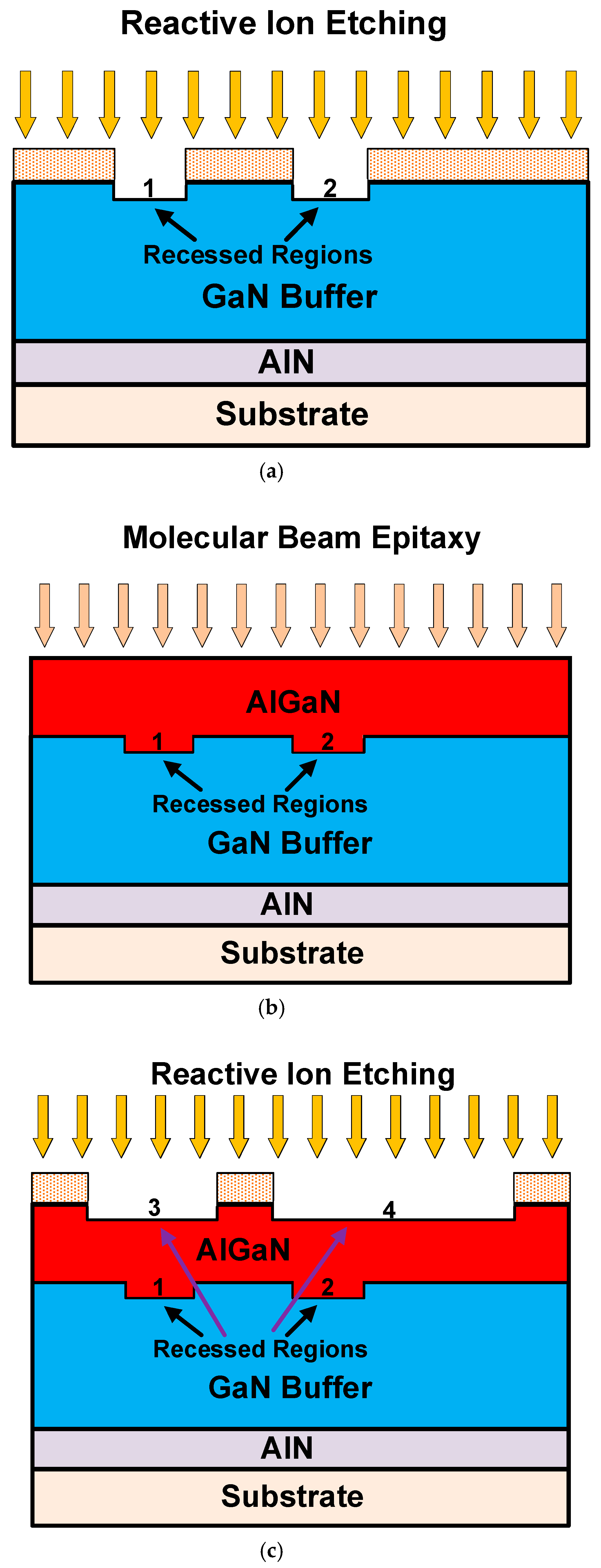
Firstly, in Figure 10 a, reactive ion etching (RIE) was used in the upper surface of the GaN layer of the device, and two recessed regions 1 and 2 were etched. CREE) announces the availability of a leading-edge process design kit (PDK) for GaN HEMT process technology. MMIC « PROCESS FLOW « AlGaN/GaN/Si.
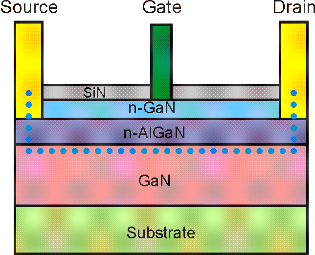
TCAD-based Model Extraction Flow for GaN HEMT Devices – Part 2. To realize cost-effective GaN power ICs, various peripheral devices should be integrated with power devices at minimum additional process complexity/cost. No junctions to deplete (un-doped) Si High mob GaN S D Source Gate Drain GaN Al Ga N x 1-x P.
A Combination of high power density, high efficiency, and wide bandwidth ;. The GSB from GaN Systems is a GaN-on-silicon HEMT transistor packaged in the GaNpx embedded die package. (d) Released AlGaN/GaN HEMT post-XeF.
"GaN is becoming more and more important in the industry. This will include generating I-V and C-V data through TCAD device simulations. The process starts with a low-temperature GaN nucleation layer, followed by an underlying C-GaN layer grown on c-face (0001) 2 in.—diameter patterned sapphire substrate 11.
Material quality Available HVS:. ©18 by SystemPlusConsulting | GaNSystemsGSB 1 22 bd Benoni Goullin 440 NANTES - FRANCE +33 2 40 18 09 16 info@systemplus.fr www.systemplus.fr GaN Systems GSB 100V 45A GaN Transistor Power Semiconductor report by ElenaBarbarini May 18 – sample REVERSECOSTING®– STRUCTURAL,PROCESS. Physics-Based Multi-Bias RF Large-Signal GaN HEMT Modeling and Parameter Extraction Flow Abstract:.
This will include a review of the current SPICE compact models for GaN HEMT devices, with a discussion of Verilog-A and simulator built-in models. Innoscience is a new entrant in the GaN-on-Silicon transistor market, with its world-first 8-inch wafer production line. Affect their process and are suitable to the processing flow.
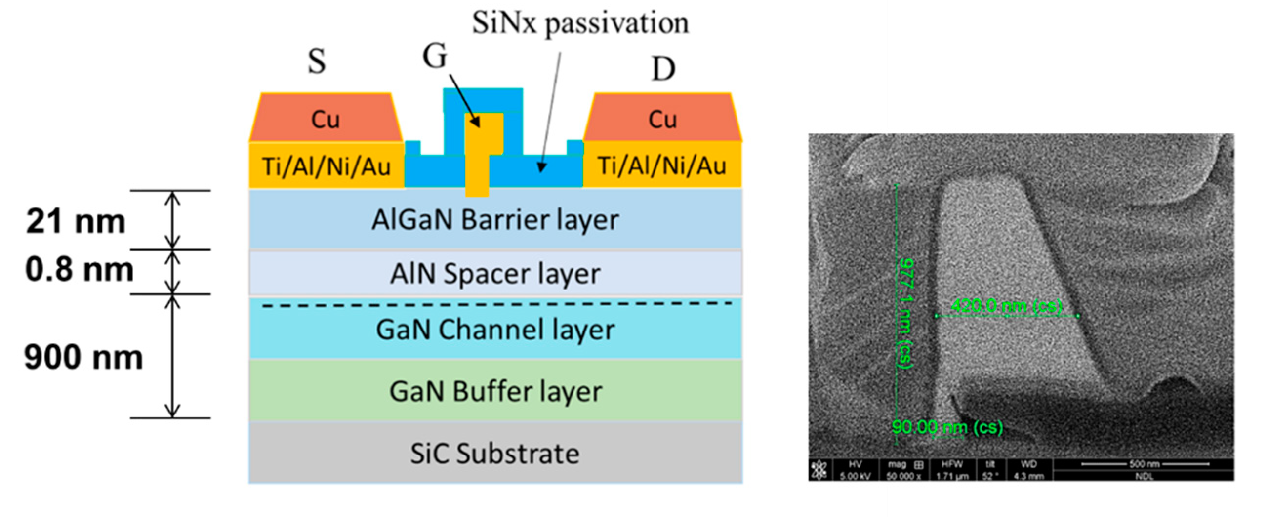
The epitaxial AlGaN/GaN heterostructure used for fabricating the FPL HEMT was grown on 6-in (111) silicon substrate by metal organic chemical vapor deposition (MOCVD). Process flow for fabrication of protected and passivated AlN/GaN MOS-HEMTs using the gate wrap-around technique. The process starts with a GaAs buffer layer epitaxially grown to isolate defects from the substrate and provide a.
A controller for generating a control signal to alternate the semiconductor switch between a turned-on state and a turned-off state;. Wide band-gap GaN HEMT;. Process main features GH25 GaN process is optimized for high power amplification up to GHz.
The report also proposes a comparison with the GaN Systems GSB 650V HEMT. This webinar will present a model parameter extraction methodology for GaN HEMT devices. Xxx contact •xxx.
Um Ga N/Diamond HEMTs was fabricated with high. A heterojunction) as the channel instead of a doped region (as is generally the case for a MOSFET).A commonly used material combination is GaAs with AlGaAs, though there. The AlN insulates the GaN layers from the silicon substrate and is the nucleation layer for the next layer.
The input data for the model extraction is generated using TCAD device simulations. 1,2,3 Propel 0mm 300mm ALD HVS:. The report provides an estimation.
F.r.:1 flow rate:5 flow rate:5 Temperature (o C) Time (S) You can use file name of 850PY, 800PY. The silicon substrate is a carrier substrate and has no function in the transistor. Ever, GaN-based HEMTs meet the demand of reduction in dynamic on-resistance, which is so-called “current collapse” phenomenon during the high power switching.
A current source for. 42) The high-voltage p-GaN gate HEMT can serve as the power switch. GaN HEMT/Si( C ) P(M)HEMT/GaAs Process Roadmaps D004GH.
The power density combined with a thermal dissipative SiC substrate reaches 4W/mm. Before run the process, check the parameters of the recipe. A recessed gate structure has been widely studied as a way to realize normally-off operation in GaN, InP, and GaAs-based HEMTs.
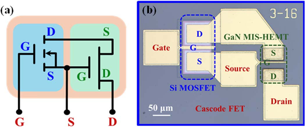
The report also proposes a comparison with the GaN Systems GSB 650V HEMT. Modifying the process flow to a lter the internal stress es can impact other characteristics of the device Therefore mechanical wafer bending is fundamental in performing controlled stress. The TPH36PS combines a normally-on GaN-on-silicon HEMT, which withstands high voltages, and a standard low voltage MOSFET, which drives high frequency, in a cascode configuration that ultimately.
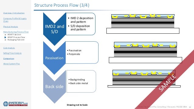
EPC GaN Transistor - Process Flow A thin layer of AlN is deposited on the silicon substrate. Temperature o hmic alloying,. Manufacturing Process Flow o HEMT Fab Unit o HEMT Process Flow o ICs Fab Unit o ICs Process Flow o Component Packaging Cost Analysis Selling Price Analysis Comparison Related Reports About System Plus GaN Transistor - Process Flow (2/4) xx for xx contact •Xxx pattern and etching SiN layer •SiN deposition and patterning.
Using a standard GaN/SiC HEMT s process procedure, 0.5. Platinum (Pt/Ti/Pt/Au) gate contact of AlGaN/GaN high electron mobility transistor (HEMT) with low gate leakage current is demonstrated. Veeco GaN HEMT Process Solutions 16 GaNHEMT Process Flow Substrate Epitaxy MSEA Gate S/D Metal GaN on Si (150mm, 0mm, 300mm) GaN on SiC (100mm, 150mm) MOCVD Dielectric Deposition HVS:.
Differing from the conventional HEMT process, a high gate and a multi-recessed buffer should be grown in the process below. 3 Standard GaN/Diamond HEMT s process Flow. The use of developed process (Cl 2 /Ar/O 2 flow of 45/10/4 sccm, p = mTorr, P RIE /P ICP = 25 W/10 W) allowed to obtain very smooth etched surface morphology and allows to fabricate normally-off AlGaN/GaN HEMTs with TiN/p-GaN gate with parameters close to the best reported in the literature 3,11,13,14,26,27.
100nm et 60nm GaN HEMTs to replace GaAs PHEMTs thanks to. Processing includes (a) sample cleaning and deoxidation, (b) 2 nm Al deposition, (c) etching Ohmic regions and thermal oxidation of Al, (d) Ohmic metallisation and annealing, and (e) gate metallisation and device measurements. This comparison highlights the huge differences in design and manufacturing process and their impact on device size and production cost.
CiteSeerX - Document Details (Isaac Councill, Lee Giles, Pradeep Teregowda):. Fully compatible with state-of-the-art GaN MMIC process 5. The Power GaN market is expected to reach $700M in 25, up from $24M in 19, driven by consumer applications, according to Yole Développement.
Home > Pure-play Wafer Foundry > Technology > GaAs & GaN RF Technologies> GaAs PHEMT > 0.25um D-Mode T-Gate PHEMT Power Process 0.25um D-Mode T-Gate PHEMT Power Process This 0.25um low cost D-Mode T-Gate process has been developed using low cost optical stepper lithography for transceiver components of up to 40 GHz and also for high operating. 3 (a) Fabricated AlGaN/GaN HEMTs in stretchable geometries. A GaN-on-Sapphire HEMT Process Flow Example ③Deposit S/D metal Ø Deposit ohmic contacts on top of AlGaN as source and drain Sapphire Substrate Buffer GaN AlGaN S D ④Lift-off and Anneal Ø To improve contact quality Ø Bad annealing may dramatically degrade the device performance ⑤Mask 03 –Gate Ø Definegateregion Ø Thealignmentinthisstepis.
Stars Library Ucf Edu Cgi Viewcontent Cgi Article 7690 Context Etd
Revisiting The Seminal Apa Optics Gan Hemt Patent Techinsights
2d Materials As Semiconducting Gate For Field Effect Transistors With Inherent Over Voltage Protection And Boosted On Current Npj 2d Materials And Applications
Indian Institute Of Science

Algan Gan Hemts Versus Inaln Gan Hemts Fabricated By150 Nm Y Gate Process Semantic Scholar
Fujitsu Develops World S First Gallium Nitride Hemt For Power Supply

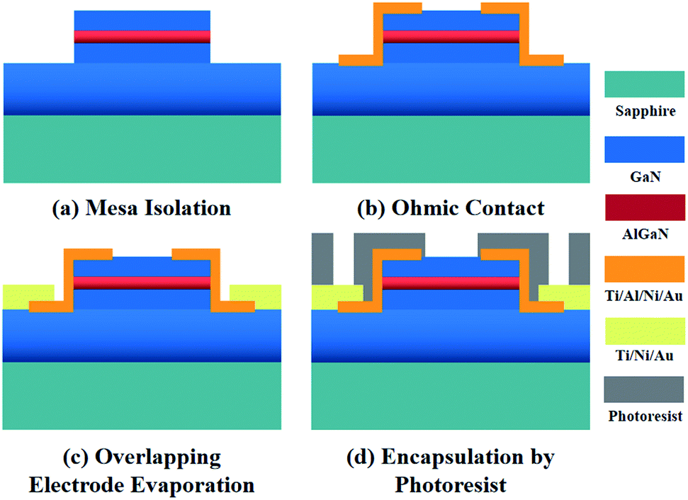
Process Flow For Fabrication Of Protected And Passivated Aln Gan Download Scientific Diagram

Stress Induced By Intrinsically Strained Silicon Nitride Passivation Films Of Algan Gan Hemts Using Victory Process 2d

Gan Stmicroelectronics
Http Citeseerx Ist Psu Edu Viewdoc Download Doi 10 1 1 1012 8152 Rep Rep1 Type Pdf
Gan Hemt
Http Iganpower Com Wp Content Uploads 19 10 Gan Power Device Tutorial Part1 Gan Basics Pdf

Ic Design In Ads Introductory Layout Training In 0 25 Um Gan Hemt Ic Process Youtube
Www Mdpi Com 1996 1944 12 10 1599 Pdf Vor

A Schematic Cross Section And Dimensions Of The Hemts B Device Download Scientific Diagram
Snfexfab Stanford Edu Sites G Files Sbiybj8726 F Sections Diplayfiles Engr241 Final Report Sj Al 1819win Pdf
Iopscience Iop Org Article 10 1149 2 jss Pdf
2

Color Online Cross Sectional Schematic Of Algan Gan Hemt Fabrication Download Scientific Diagram
Http Www Inrel Npower Eu Sites Default Files T05 Meneghesso Reliability Phd Brixen Jul 17 Pdf
Http Www Inrel Npower Eu Sites Default Files T05 Meneghesso Reliability Phd Brixen Jul 17 Pdf
Gan Sic Based High Electron Mobility Transistors For Integrated Microwave And Power Circuits

Aln Gan Based Mos Hemt Technology Processing And Device Results
Www Systemplus Fr Wp Content Uploads 18 04 Sp165 Gan On Silicon Transistor Comparison Sample 3 Pdf
Compoundsemiconductor Net Article Making Waves With The Gan Hemt Feature
Gan Hemt On Silicon Wafers Universitywafer Inc

Moscap And Hemt Process Flows A Moscap Process Flow N Gan Substrate Download Scientific Diagram
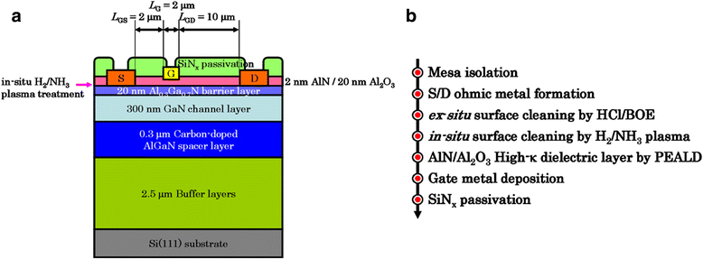
Figure 1 Aln Surface Passivation Of Gan Based High Electron Mobility Transistors By Plasma Enhanced Atomic Layer Deposition Springerlink
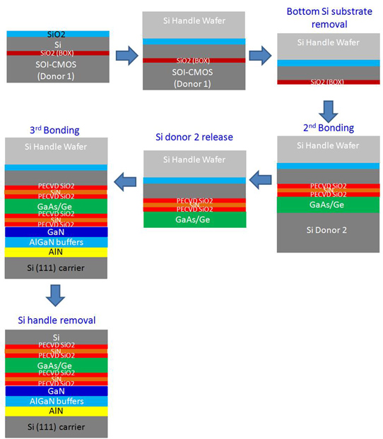
Wafer Bonding To Integrate Silicon Gallium Arsenide And Gallium Nitride

Device With Process Simplification And Ar Pretreatment Of Al2o3 Before F Plasma Treatment To Create Deeper Electron Traps For High Temperature Operation Power Microelectronics Device And Process Technologies
Http Ssie Dei Unipd It Wp Content Uploads 17 07 T01 Moens Ganhemts Phd Brixen Jul 17 Pdf

Exposing Pollutants With Gan Hemts News
Electronics Free Full Text A Comprehensive Review Of Recent Progress On Gan High Electron Mobility Transistors Devices Fabrication And Reliability Html
A Sandwich Structured Algan Gan Hemt With Broad Transconductance And High Breakdown Voltage Journal Of Materials Chemistry C Rsc Publishing
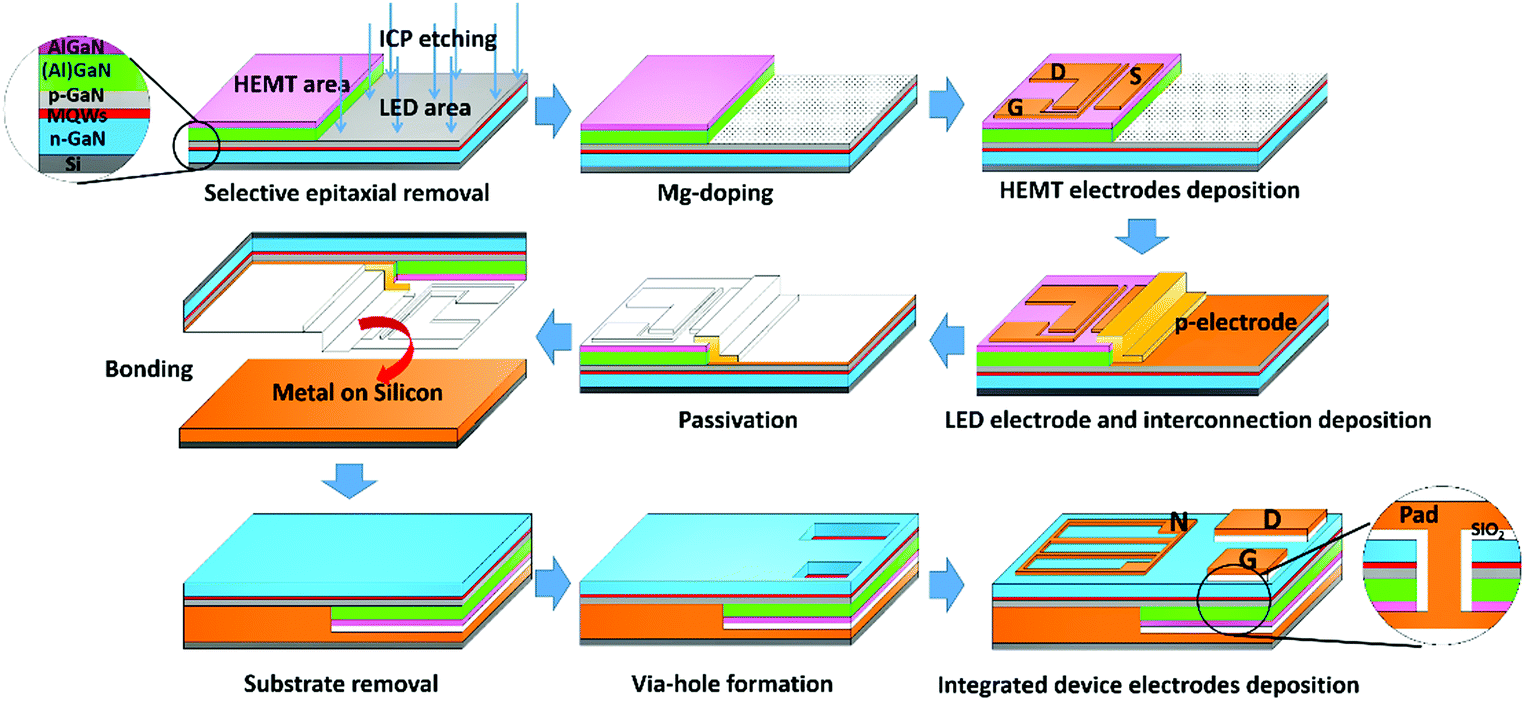
Efficiency Improved By Monolithic Integration Of Hemt With Vertical Structure Leds And Mg Doping On Dry Etched Gan Journal Of Materials Chemistry C Rsc Publishing

Schematics Showing The Process Flow Of E D Mode Hemts A Ohmic Download Scientific Diagram

Performance Optimization Of Lateral Algan Gan Hemts With Cap Gate On 150 Mm Silicon Substrate Sciencedirect
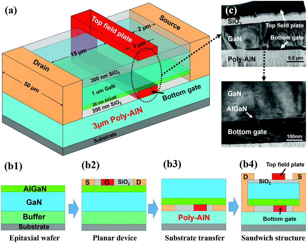
A Sandwich Structured Algan Gan Hemt With Broad Transconductance And High Breakdown Voltage Journal Of Materials Chemistry C Rsc Publishing
Mantech Presentation V1
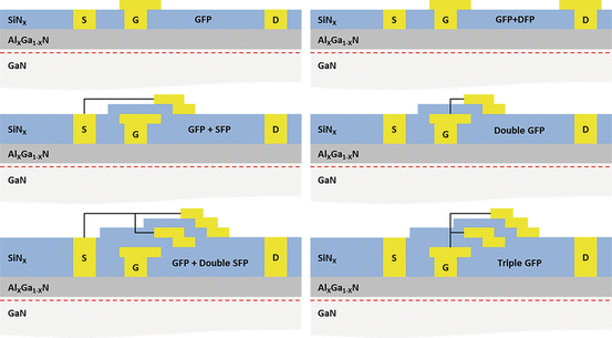
Micromachines Free Full Text Novel High Energy Efficiency Algan Gan Hemt With High Gate And Multi Recessed Buffer Html
Gallium Nitride Developments In India Full Afterburner
Tcad Based Gan Hemt Scalable Modeling Flow Using The Mvsg Compact Model Silvaco

Schematics Showing The Process Flow Of The Ln Zno Algan Gan Hemts A Download Scientific Diagram

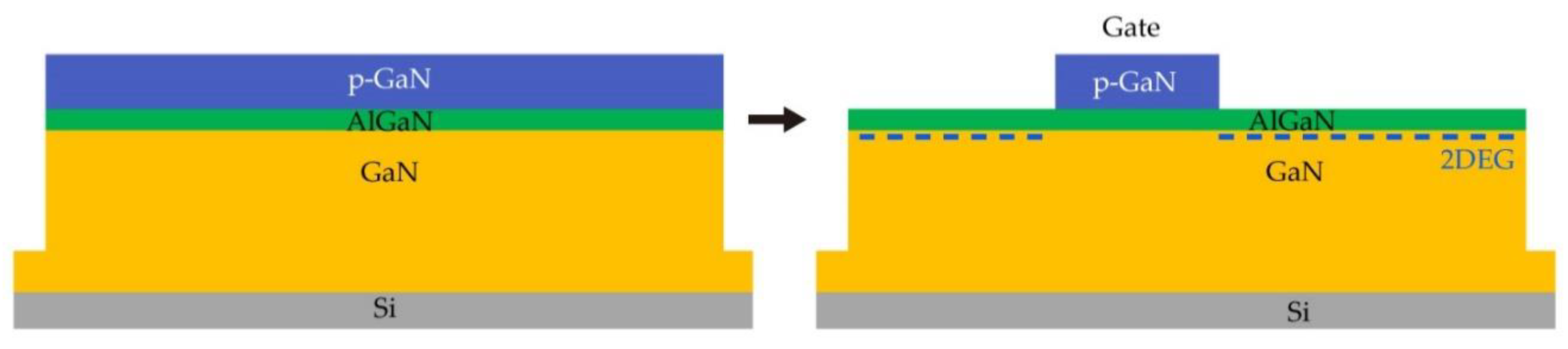
Review Of Technology For Normally Off Hemts With P Gan Gate Sciencedirect
Fujitsu Develops World S First Gan Hemt Able To Cut Power In Standby Mode And Achieve High Output
Boron Nitride Releases Gan Transistors From Self Heating Degradation

Schematic Of The Updated Process Flow To Realize The Integrated Sicmos Download Scientific Diagram
Dspace Mit Edu Bitstream Handle 1721 1 Palacios Gan On Si technology Pdf Sequence 1 Isallowed Y
Thermal Management Of Gan On Si High Electron Mobility Transistor By Copper Filled Micro Trench Structure Scientific Reports

Color Online Epilayer Grown And Process Flow Of The Studied Download Scientific Diagram

Novel Junction Level Cooling In Pulsed Gan Devices

Gan Power Devices The Hemt Youtube

Moscap And Hemt Process Flows A Moscap Process Flow N Gan Substrate Download Scientific Diagram
Lateral Gan Hemt Structures Springerlink
2

Effect Of Surface Passivation Process For Algan Gan Hemt Heterostructures Using Phenol Functionalized Porphyrin Based Organic Molecules Journal Of Applied Physics Vol 124 No 19
Www Systemplus Fr Wp Content Uploads 18 04 Sp165 Gan On Silicon Transistor Comparison Sample 3 Pdf
2

Figure 3 From Monolithically Integrated Enhancement Depletion Mode Algan Gan Hemt Inverters And Ring Oscillators Using Hboxcf 4 Plasma Treatment Semantic Scholar
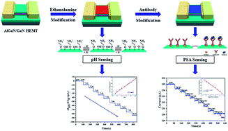
Highly Sensitive Algan Gan Hemt Biosensors Using An Ethanolamine Modification Strategy For Bioassay Applications Rsc Advances Rsc Publishing
Q Tbn 3aand9gcsrmh6hxn2xcbtvnht2hdks4ohqsytrioqtpw Usqp Cau

Performance And Reliability Of Algan Gan Hemt On Cs Mantech
Onlinelibrary Wiley Com Doi Pdf 10 1002 Pssa

Color Online Flowchart Of Backside Processing Of The Gan Hemt On A Download Scientific Diagram

Figure 3 From 1 6kv 2 9 Mw Cm2 Normally Off P Gan Hemt Device Semantic Scholar
Transfer Printing And Self Aligned Etching For E Mode Gan Transistors

Diamond Thermal Management Boosts Output Power Of Inalgan Transistor
Http Iganpower Com Wp Content Uploads 19 10 Gan Power Device Tutorial Part1 Gan Basics Pdf
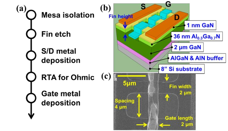
Investigation Of Gan Fin Hemts With Micron Scale Fin Width
Panasonic 600 V Gan Hemt Pga26e19ba 17 Teardown Reverse Costing Rep

Figure 1 From New Fabrication Process To Manufacture Rf Mems And Hemt On Gan Si Substrate Semantic Scholar
Www Mdpi Com 72 666x 11 1 53 Pdf
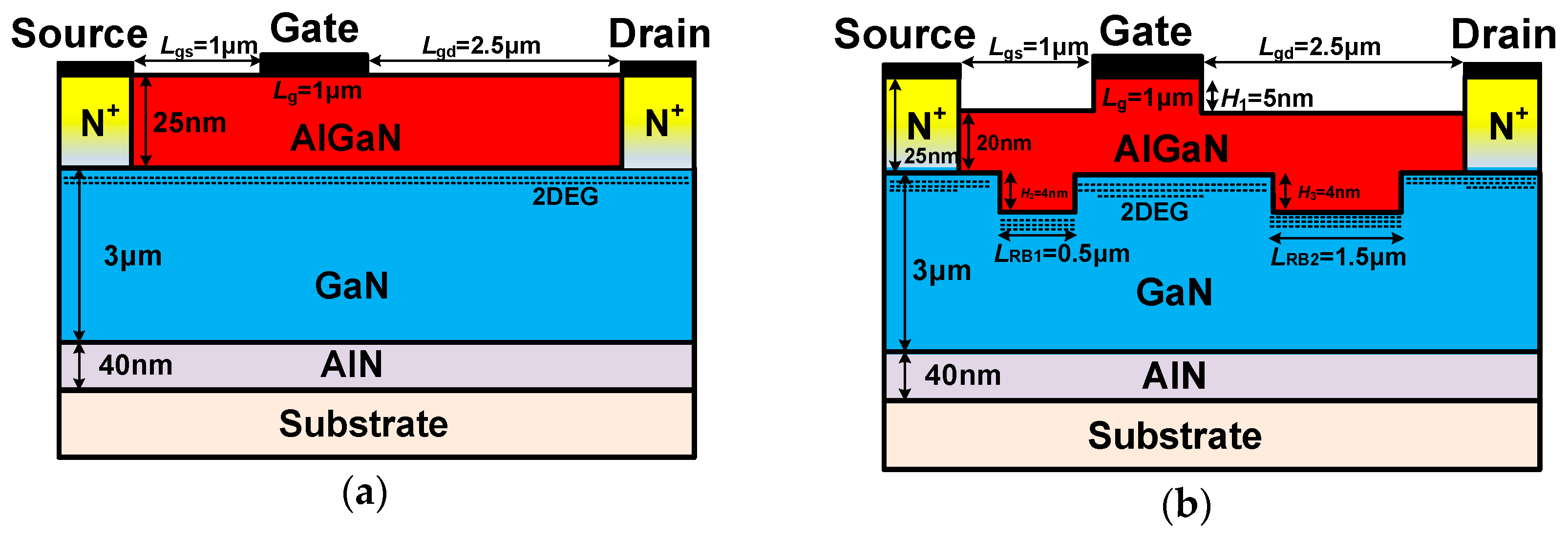
Micromachines Free Full Text Novel High Energy Efficiency Algan Gan Hemt With High Gate And Multi Recessed Buffer Html
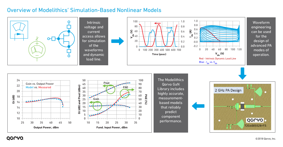
Gan Hemt Models 101 How Do Nonlinear Models Help With Gan Pa Design Qorvo
Novel Of Normally Off Gan Hemt Device Structure By Cs Mantech
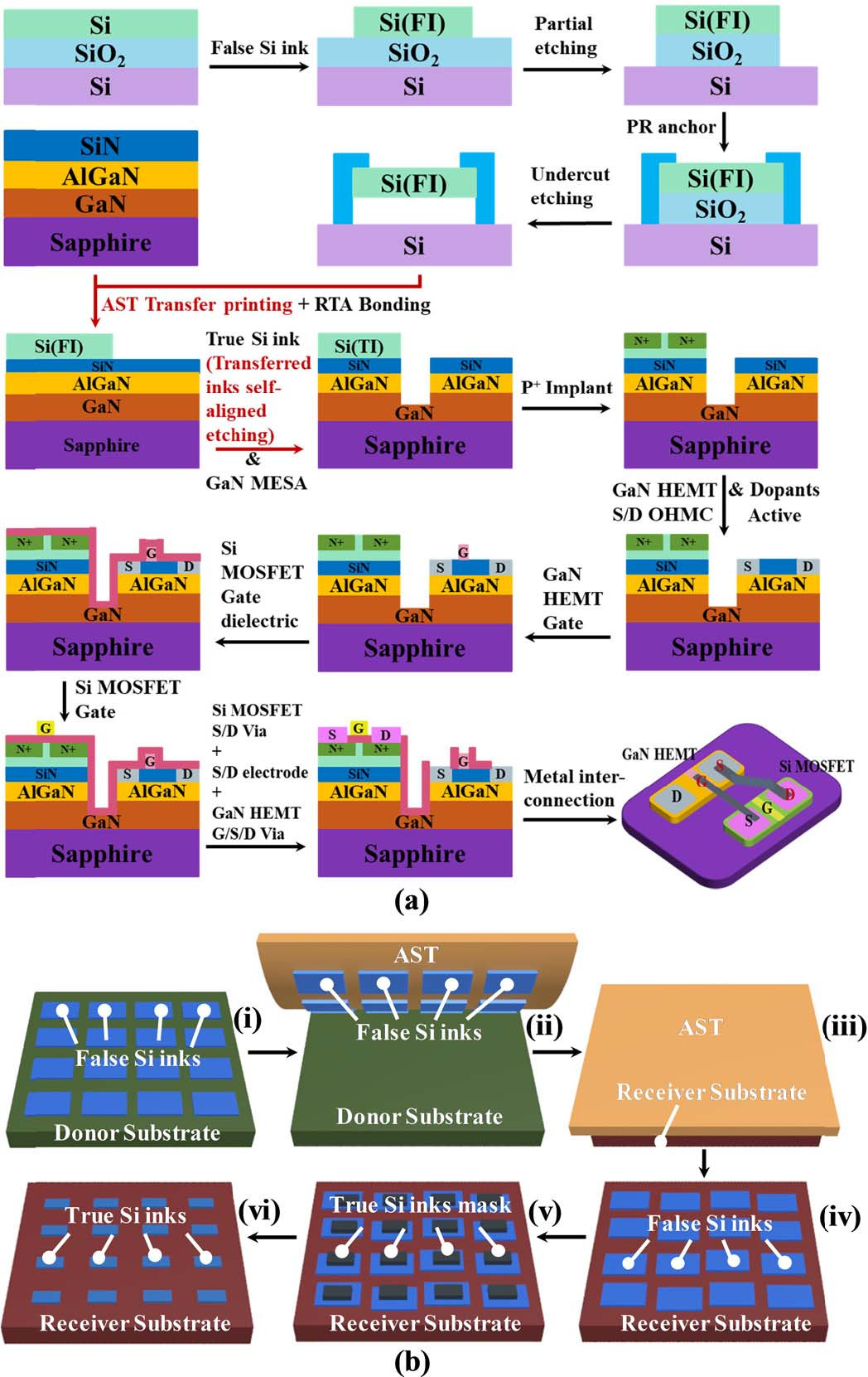
Transfer Printing And Self Aligned Etching For E Mode Gan Transistors

Figure 3 From Monolithic Integration Of G Semantic Scholar
Ieeexplore Ieee Org Iel7 0657 Pdf

Review Of Technology For Normally Off Hemts With P Gan Gate Sciencedirect
Electronics Free Full Text A Comprehensive Review Of Recent Progress On Gan High Electron Mobility Transistors Devices Fabrication And Reliability Html
Electronics Free Full Text A Comprehensive Review Of Recent Progress On Gan High Electron Mobility Transistors Devices Fabrication And Reliability Html
Transphorm Gan On Silicon Hemt Tph36ps 16 Teardown Reverse Costin

3d Gan Nanoarchitecture For Field Effect Transistors Sciencedirect

Comparative Analysis Of Parameter Extraction Techniques For Algan Gan Hemt On Silicon Sapphire Substrate Sciencedirect
Revisiting The Seminal Apa Optics Gan Hemt Patent Techinsights
Ieeexplore Ieee Org Iel7 0657 Pdf

Review Of Technology For Normally Off Hemts With P Gan Gate Sciencedirect
Low Leakage Gan Hemts With Sub 100 Nm T Shape Gates Fabricated By A Low Damage Etching Process Springerlink

Schematic Views Of The Process Flow For Micro Trench Fabrication In Download Scientific Diagram
Scholarworks Rit Edu Cgi Viewcontent Cgi Article 1568 Context Ritamec

The Process Flow Of The Heterogeneous Integration Of Gan With Si 100 Download Scientific Diagram
Http Www Inrel Npower Eu Sites Default Files T05 Meneghesso Reliability Phd Brixen Jul 17 Pdf
Stacking Gan And Silicon Transistors On 300 Mm Silicon News
Gan Sic Based High Electron Mobility Transistors For Integrated Microwave And Power Circuits


